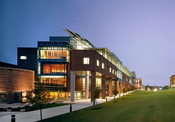


More than 145 programs at the bachelor's,
master's, and doctoral levels

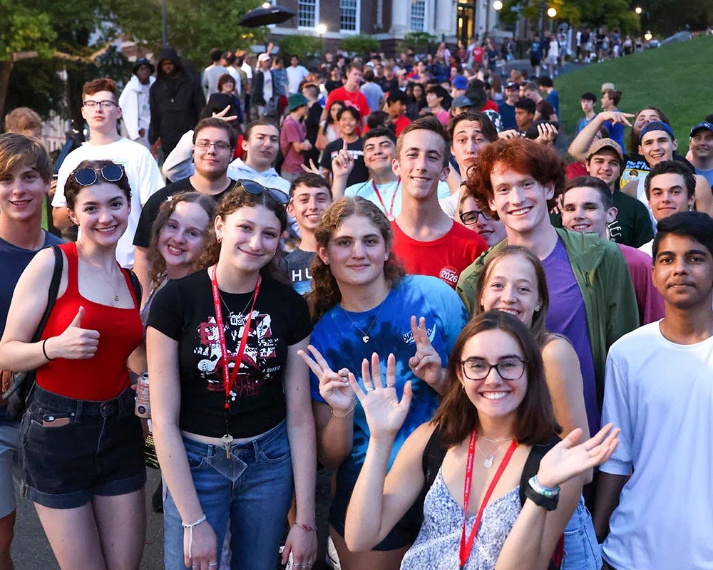
What's your RPI first? What's your defining moment? Share your journey and unforgettable memories. Be part of RPI's legacy.


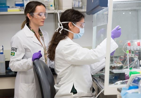
Want to fast-track your MD? Take part in RPI and AMC’s accelerated Physician Scientist program!
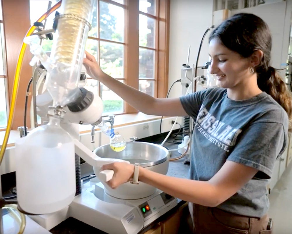
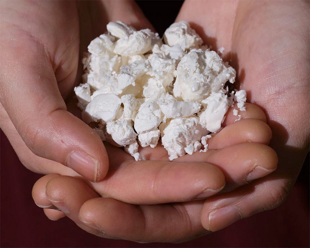
Move over Spider-Man:
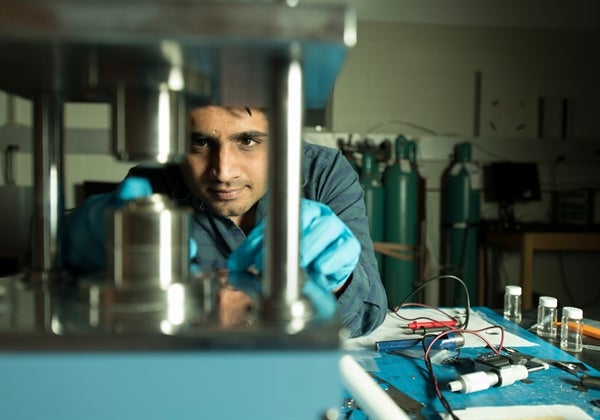
Our researchers have developed a strain of bacteria that can turn plastic waste into biodegradable spider silk.
Our researchers have developed a strain of bacteria that can turn plastic waste into biodegradable spider silk.