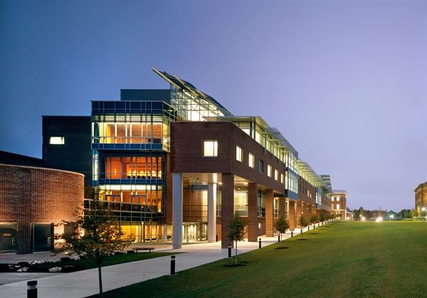


More than 145 programs at the bachelor's,
master's, and doctoral levels

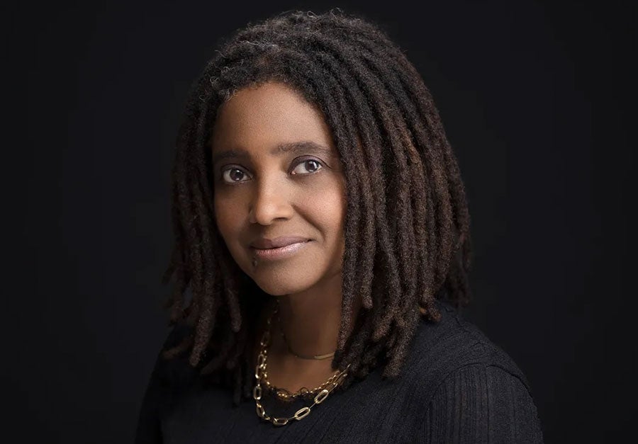
Former U.S. Poet Laureate Tracy K. Smith To Be Guest Speaker at 83rd McKinney Award Ceremony
April 19 at 7 p.m.
April 19 at 7 p.m.

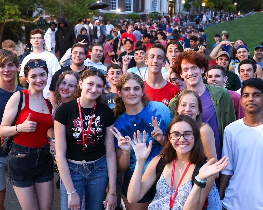
What's your RPI first? What's your defining moment? Share your journey and unforgettable memories. Be part of RPI's legacy.

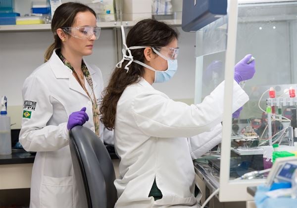
Want to fast-track your MD? Take part in RPI and AMC’s accelerated Physician Scientist program!
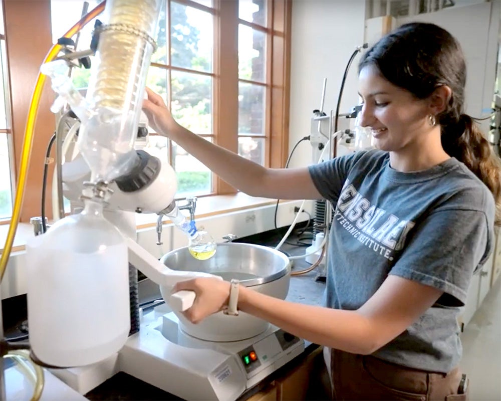
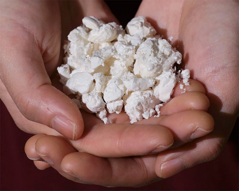
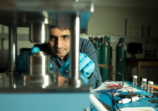
Move over Spider-Man:
Our researchers have developed a strain of bacteria that can turn plastic waste into biodegradable spider silk.
Our researchers have developed a strain of bacteria that can turn plastic waste into biodegradable spider silk.